
This is a reference size drawing of the PC board printed circuit board of the SOT773-1 type produced by Philips Semiconductors
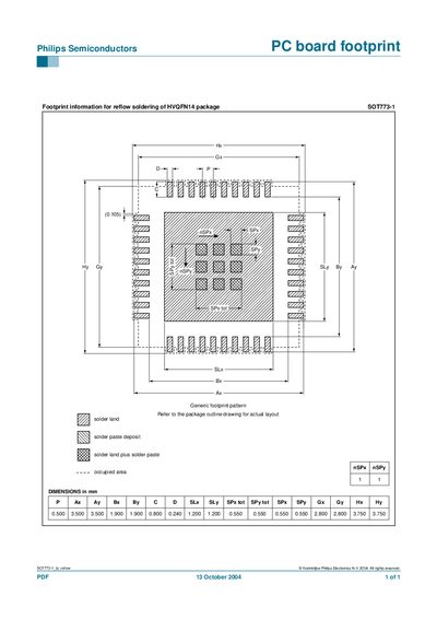
This document supplies the printed‑circuit‑board (PCB) footprint information for the Philips SOT773-1 semiconductor package, which uses an HVQFN14 lead‑frame. It includes the generic footprint pattern, pad dimensions, and recommended solder paste deposition.
The table lists key mechanical dimensions such as pad pitch, pad length, and solder land sizes in millimetres, allowing designers to create accurate PCB layouts for reflow soldering of the component.
| Pad pitch (Px) | 0.500 mm |
|---|---|
| Pad length (Ax) | 3.500 mm |
| Pad width (Ay) | 3.500 mm |
| Solder land length (SLx) | 0.800 mm |
| Solder land width (SLy) | 0.240 mm |
The footprint is for the HVQFN14 package of the SOT773-1 component.
It was published on 13 October 2004.