
This document provides PCB footprint dimensions for SOT481-2. For more details, please refer to the document content.
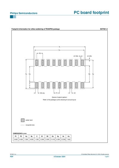
This document supplies the PCB footprint information required for reflow soldering of the Philips SOT481-2 (TSSOP56) semiconductor package. It includes a generic footprint pattern and references to the package outline drawing for exact layout.
The key dimensions are listed in millimetres for pads, land patterns, and overall package size, enabling accurate board design and manufacturing.
| P1 | 0.400 mm |
|---|---|
| P2 | 0.430 mm |
| Ay | 7.200 mm |
| By | 4.500 mm |
| C | 1.350 mm |
| D1 | 0.240 mm |
| D2 | 0.300 mm |
| Gx | 11.410 mm |
| Gy | 5.300 mm |
| Hx | 13.300 mm |
| Hy | 7.450 mm |
The footprint dimensions are P1 0.400 mm, P2 0.430 mm, Ay 7.200 mm, By 4.500 mm, C 1.350 mm, D1 0.240 mm, D2 0.300 mm, Gx 11.410 mm, Gy 5.300 mm, Hx 13.300 mm, and Hy 7.450 mm.
The SOT481-2 footprint corresponds to the TSSOP56 package.