
This document is the PCB footprint information for SOT662-1
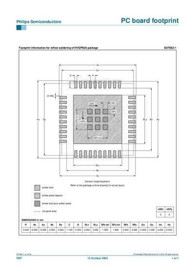
This document provides the printed‑circuit‑board (PCB) footprint data required for reflow soldering of the HVQFN20 package identified as SOT662-1. It includes the generic footprint pattern and the recommended dimensions for pads, solder paste, and occupied area.
The table lists key dimensions in millimetres, such as pad pitch, pad length, and pad width, together with the total solder land and paste areas. Designers should refer to the package outline drawing for the exact layout before applying these values.
It applies to the HVQFN20 package SOT662-1.
The manual was published on 13 October 2004.
© Koninklijke Philips Electronics N.V. 2004.