
This is a reference document for the PCB footprint of SOT807-1. It provides information such as the size of the PCB, the size of the solder pad, and the occupied area of the solder paste.
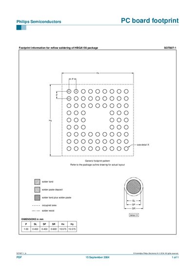
This document supplies the PCB footprint data required for reflow soldering of the HBGA156 package identified as SOT807-1. It lists the pad, solder land, solder paste deposit, and solder resist dimensions, as well as the overall footprint size.
The generic footprint pattern and detailed dimensions are given in millimetres, and users are directed to the package outline drawing for the exact layout of the component on a board.
| Package type | HBGA156 |
|---|
The footprint includes a 1.00 mm pad, 0.450 mm solder land and paste widths, a 0.600 mm solder resist, and overall dimensions of 15.575 mm × 15.575 mm.
Refer to the package outline drawing for the actual layout.