
SOT543-1_fp is the PCB footprint dimensions for Philips Semiconductors SOT543-1 chip
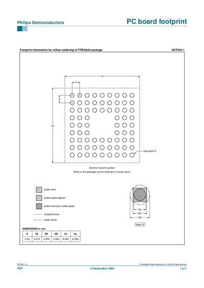
This document provides the PCB footprint information for the Philips SOT543-1 surface‑mount package, intended for reflow soldering. It includes a generic footprint pattern and references the package outline drawing for the exact layout.
Key dimensions are listed in millimetres, covering pad length, pad spacing, pad width, solder resist area, and overall footprint size. The data helps designers create correct land patterns for reliable assembly.
| Pad length (P) | 0.50 mm |
|---|---|
| Pad spacing (SL) | 0.275 mm |
| Pad width (sP) | 0.300 mm |
| Solder resist width (SR) | 0.425 mm |
| Footprint X dimension (Hx) | 6.500 mm |
| Footprint Y dimension (Hy) | 6.500 mm |
The document shows a generic footprint pattern that should be used, referencing the package outline drawing for the exact layout.
The footprint dimensions are: pad length 0.50 mm, pad spacing 0.275 mm, pad width 0.300 mm, solder resist width 0.425 mm, overall X and Y dimensions 6.500 mm each.