
This document is about the dimensions of Philips Semiconductors PC board footprint SOT684-1
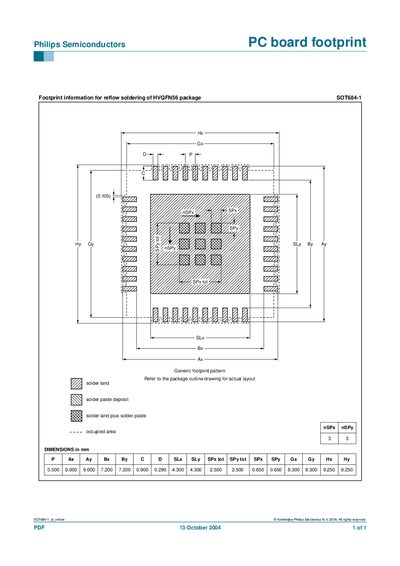
This document provides the printed‑circuit‑board (PCB) footprint data required for reflow soldering of the Philips SOT684-1 HVQFN56 semiconductor package. It includes the generic footprint pattern, pad dimensions, and solder paste recommendations.
The layout references the package outline drawing for the exact geometry. Key dimensions such as overall package size (9.000 mm × 9.000 mm) and pad sizes are listed in millimetres.
| Package overall size | 9.000 mm × 9.000 mm |
|---|
The document advises to refer to the package outline drawing for the actual layout.
It includes the solder land, solder paste deposit, and the combination of solder land plus solder paste.