
This is a PDF file containing the dimensions of Philips Semiconductors PC board footprint SOT784-1, including occupied area, reflow soldering package LQFP100 footprint information, and solder land map.
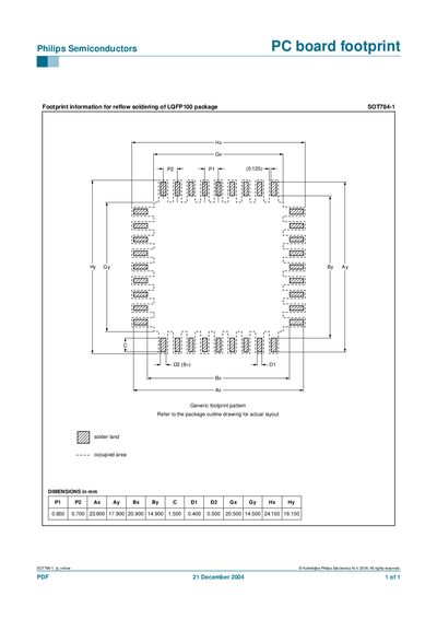
This document provides the printed‑circuit‑board (PCB) footprint for the Philips SOT784-1 LQFP100 semiconductor package. It is intended for designers who need the exact pad layout and dimensions for reflow soldering.
The generic footprint pattern lists pad coordinates (Pi, P2, AX, Ay, etc.) in millimetres, and the document refers to the package outline drawing for the actual layout. All dimensions are given in mm and are suitable for standard PCB fabrication.
It is for the LQFP100 package identified as SOT784-1.
Refer to the package outline drawing; the document lists all dimensions in millimetres.
The manual was dated 21 December 2004.