
This document provides information about the dimensions of the NXP B.V. PC board footprint SOT841-4 package, as well as the solder land information for reflow soldering.
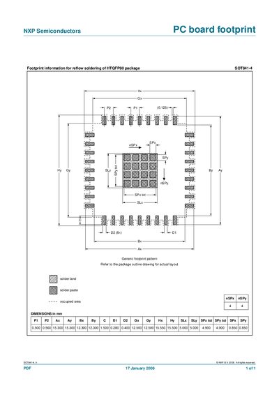
This document supplies the footprint information required for reflow soldering of the HTQFP80 SOT841-4 package. It includes the generic footprint pattern and references the package outline drawing for the exact layout.
Key dimensions such as pad pitch, pad size, and solder land spacing are listed in millimetres, enabling accurate PCB design and manufacturing for this component.
| Pad pitch (P2) | 0.500 mm |
|---|---|
| Pad width (Ax) | 0.560 mm |
| Pad length (Ay) | 15.300 mm |
| Solder land width (SLx) | 1.500 mm |
The generic footprint pattern is shown in the document and you should refer to the package outline drawing for the actual layout.
The pad pitch is 0.500 mm, pad width is 0.560 mm, and pad length is 15.300 mm as listed in the dimensions table.