
This is a PDF file. The file contains the PCB footprint dimensions information of the SOT1024-2 product.
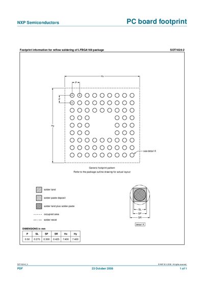
The document describes the PCB footprint required for reflow soldering of the LFBGA169 package identified as $0T1024-2. It includes a generic footprint pattern and references the package outline drawing for the exact layout.
Key dimensions are listed in millimetres, covering pad length, solder land size, and overall footprint extents. The data can be used to create accurate PCB layouts for this component.
| Pad length (P) | 0.50 mm |
|---|---|
| Pad width (SL) | 0.275 mm |
| Solder land length (sP) | 0.300 mm |
| Solder land width (SR) | 0.425 mm |
| Footprint X dimension (Hx) | 7.400 mm |
| Footprint Y dimension (Hy) | 7.400 mm |
The document provides a generic footprint pattern that should be used, with dimensions listed in the dimensions table.
Pad length is 0.50 mm, pad width is 0.275 mm, solder land length is 0.300 mm, and solder land width is 0.425 mm.