
This document is the printed circuit board footprint dimensions information for SOT911-1 chip.
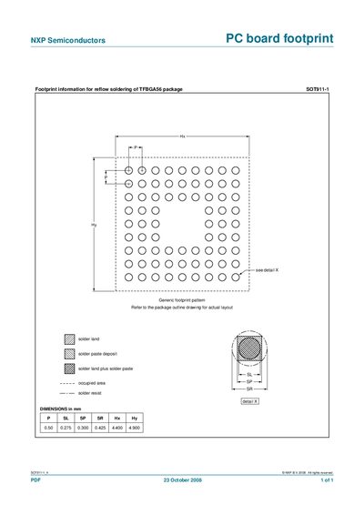
This document provides the PCB footprint information required for reflow soldering of the NXP SOT911-1 device, which uses a TFBGA56 package. It includes the generic footprint pattern and references the package outline drawing for the exact layout.
Key dimensions such as pad length, solder land size, and solder paste deposit are listed in millimetres, along with the occupied area and solder resist guidelines to aid PCB designers in creating a compliant layout.
| Pad length (P) | 0.50 mm |
|---|---|
| Solder land length (SL) | 0.275 mm |
| Solder paste length (sP) | 0.300 mm |
| Solder resist width (SR) | 0.425 mm |
| Footprint width (Hx) | 4.400 mm |
| Footprint height (Hy) | 4.900 mm |
The SOT911-1 uses a TFBGA56 package.
The footprint dimensions are: Pad length 0.50 mm, solder land length 0.275 mm, solder paste length 0.300 mm, solder resist width 0.425 mm, overall width 4.400 mm, and height 4.900 mm.