
This document is a datasheet published by NXP Semiconductors about the PCB footprint dimensions and soldering information of the SOT994-1.
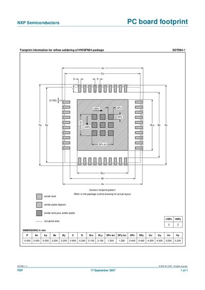
This document provides the printed‑circuit‑board (PCB) footprint data for the NXP SOT994-1 HWQFN24 package. It includes the generic footprint pattern, pad dimensions, and recommended solder paste deposition for reflow soldering.
The layout references the package outline drawing and lists all critical dimensions in millimetres, such as pad pitch, pad size, and solder land coordinates, to aid designers in creating accurate PCB footprints.
It applies to the HWQFN24 package SOT994-1.
The document was published on 17 September 2007.