
This is a footprint information for SOT728-2
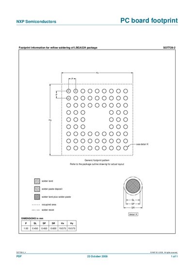
This document supplies the PCB footprint information required for reflow soldering of the LBGA324 package identified as SOT728-2. It includes the layout of solder lands, paste deposits, and the occupied area on the board.
Key dimensions such as Hx, Hy and other layout measurements are listed in millimetres, and users are directed to the package outline drawing for the complete layout details.
It corresponds to the LBGA324 package.
Refer to the package outline drawing for the actual layout.