
This document provides information about the PC board footprint dimensions for NXP Semiconductors. It includes details about the solder land dimensions, solder paste occupied area, and the footprint pattern for reflow soldering of the LFBGA487 package.
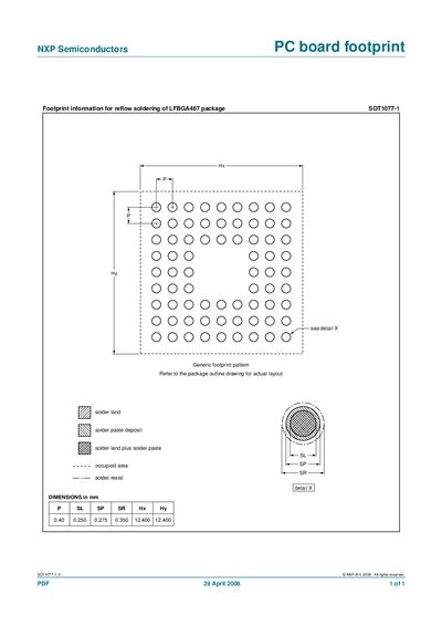
This document supplies the recommended PCB footprint for the NXP SOT1077-1 (LFBGA487) semiconductor package, including pad layout and solder paste recommendations for reflow soldering.
The footprint dimensions are listed in millimetres, and users are directed to the package outline drawing for the exact layout details.
| Pad length (P) | 0.40 mm |
|---|---|
| Pad width (SL) | 0.250 mm |
| Pad spacing (sP) | 0.275 mm |
| Pad spacing (SR) | 0.350 mm |
| Footprint height (Hx) | 12.400 mm |
| Footprint width (Hy) | 12.400 mm |
The document shows an ‘N’ solder paste deposit in the footprint diagram.
Refer to the package outline drawing for the actual layout.