
This is a document about the PCB foot print dimension of SOT999-1.
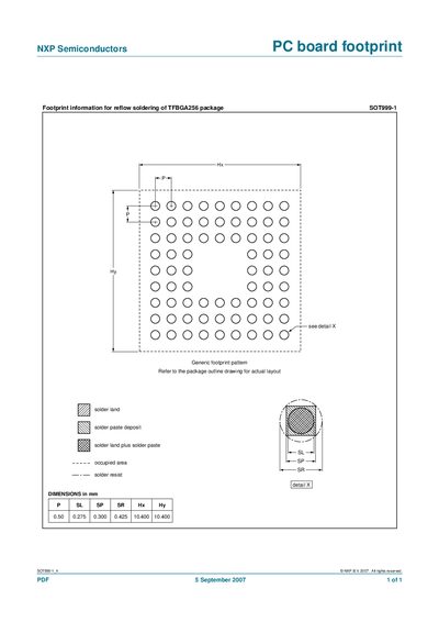
This manual supplies the generic footprint pattern and layout recommendations for the NXP SOT999-1 (TFBGA256) package, intended for use in PCB design and reflow soldering processes.
The document lists key dimensions such as pad length, solder land size, and overall footprint size, and refers to the package outline drawing for the exact layout details.
| P | 0.50 mm |
|---|---|
| SL | 0.275 mm |
| sP | 0.300 mm |
| SR | 0.425 mm |
| Hx | 10.400 mm |
| Hy | 10.400 mm |
The manual provides a generic footprint pattern and advises to refer to the package outline drawing for the actual layout.
Key dimensions are P = 0.50 mm, SL = 0.275 mm, sP = 0.300 mm, SR = 0.425 mm, Hx = 10.400 mm, Hy = 10.400 mm.