
This document is a PDF file of PCB footprint information for the electronic component SOT836-1. The document includes dimensions of the PCB board, solder lands, solder paste, and solder resist.
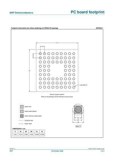
This document provides the PCB footprint layout for the NXP SOT836-1 package, which uses an LFBGA167 ball grid array. It includes the generic pattern, solder land definitions, and recommended solder paste deposit areas.
The dimensions are given in millimetres for pad length, solder land size, and overall footprint extents, and reference to the package outline drawing is provided for the exact layout.
| Pad length (P) | 0.50 mm |
|---|---|
| Solder land width (SL) | 0.275 mm |
| Solder land length (sP) | 0.300 mm |
| Solder resist width (SR) | 0.425 mm |
| Footprint X dimension (Hx) | 14.400 mm |
| Footprint Y dimension (Hy) | 14.400 mm |
It is for the LFBGA167 package SOT836-1.
The pad length is 0.50 mm, solder land width 0.275 mm, solder land length 0.300 mm, solder resist width 0.425 mm, and the overall footprint is 14.400 mm by 14.400 mm.