
This document is about the PC board footprint for reflow soldering of NXP Semiconductors XQFN8 package. The document provides dimensions and layout of the footprint, as well as the clearance placement and occupied area solder lands for soldering process.
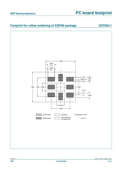
This document defines the printed‑circuit‑board (PCB) footprint for the NXP Semiconductors SOT902-1 device, which is supplied in an XQFN8 package. It is intended for designers who need the exact pad layout and clearances for reliable reflow soldering.
Key dimensions such as pad size, spacing, and overall footprint are listed in millimetres, together with recommended solder‑paste parameters. The data can be directly used to create the footprint in CAD tools or to verify existing board designs.
| Package type | XQFN8 |
|---|
The SOT902-1 is supplied in an XQFN8 package.
The overall footprint measures 1.900 mm by 0.450 mm.