
This is a PDF file containing the package dimension information of SOT630-2, including P, SL, SP, SR, etc.
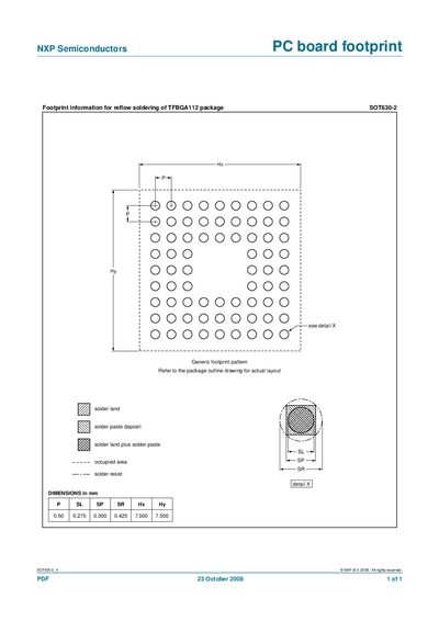
This document defines the PCB footprint for the NXP SOT630-2 (TFBGA112) package, giving the layout needed for reflow soldering. It includes a generic pattern and references the package outline drawing for the exact geometry.
Key dimensions such as pad pitch, pad length, solder resist width, and overall footprint size are listed in millimetres, allowing designers to create compliant board layouts.
| Pad Pitch (P) | 0.50 mm |
|---|---|
| Pad Length (SL) | 0.275 mm |
| Pad Width (sP) | 0.300 mm |
| Solder Resist Width (SR) | 0.425 mm |
| Height X (Hx) | 7.500 mm |
| Height Y (Hy) | 7.500 mm |
It applies to the TFBGA112 package SOT630-2.
The exact layout is shown in the package outline drawing referenced in the document.
The footprint dimensions are P=0.50 mm, SL=0.275 mm, sP=0.300 mm, SR=0.425 mm, Hx=7.500 mm, Hy=7.500 mm.