
This document describes the PCB board footprint for reflow soldering of the HSOP16F package produced by NXP B.V. in 2008. The document provides the dimensions and solder pad layout of the package.
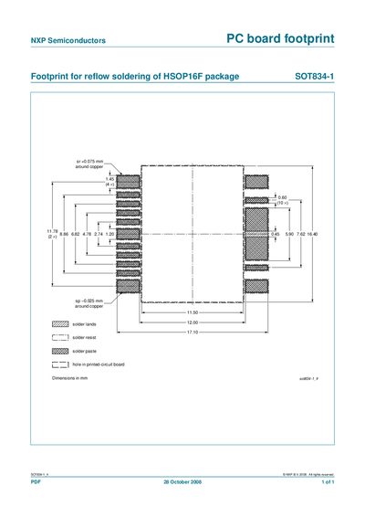
This document describes the printed‑circuit‑board (PCB) footprint for the NXP SOT834-1 component. It is intended for designers who need to place the HSOP16F package on a board and apply appropriate soldering processes.
Key details include the overall dimensions, recommended solder paste and resist layers, and hole specifications. The footprint data are expressed in millimetres and conform to NXP's 2008 design guidelines.
| Dimensions (mm) | 5, 5.90, 7.62, 16.40 |
|---|---|
| Package Type | HSOP16F |
The SOT834-1 uses the HSOP16F package.
The footprint dimensions are 5 mm, 5.90 mm, 7.62 mm, and 16.40 mm.
It was published on 28 October 2008.