
This document provides information on the dimensions and soldering details of the NXP Semiconductors PC board footprint SOT815-1. It includes the footprint information for reflow soldering of the DHVQFN24 package.
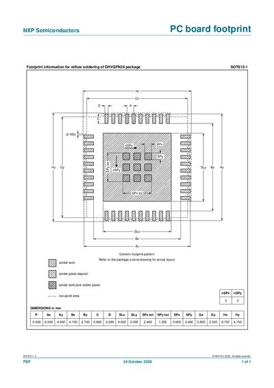
This document supplies the PCB footprint information required for reflow soldering of the DHVQFN24 package SOT815-1. It includes generic footprint patterns, solder land definitions, and references to the package outline drawing for the actual layout.
Key dimensions are listed in millimetres, covering pad sizes, spacing, and occupied area. The data enables designers to correctly place and size solder pads for reliable assembly of the component.
| Pad X (Px) | 0.500 mm |
|---|---|
| Pad Y (Py) | 6.500 mm |
| Pad width (Ax) | 4.500 mm |
| Pad height (Ay) | 4.700 mm |
| Solder land spacing (SLx) | 0.900 mm |
It applies to the DHVQFN24 package SOT815-1.
Refer to the package outline drawing for the actual layout.