
SOT762-1 PC board footprint for reflow soldering of DHVQFN14 package
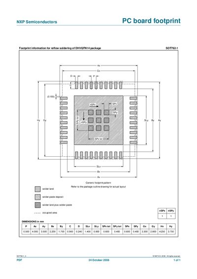
This document supplies the recommended PCB footprint for the NXP SOT762-1 DHVQFN14 package, including pad layout, solder paste deposit areas, and occupied area dimensions. It is intended for use in reflow soldering processes.
The generic footprint pattern is listed with exact dimensions in millimetres, and users are directed to the package outline drawing for the final layout. All dimensions are given in a table format for quick reference.
| Pad pitch X (mm) | 0.500 |
|---|---|
| Pad pitch Y (mm) | 4.000 |
It applies to the DHVQFN14 package SOT762-1.
Refer to the package outline drawing for the actual layout.