
This is a file about the PCB footprint of SOT510-1, which describes its dimensions, location and soldering method in detail.
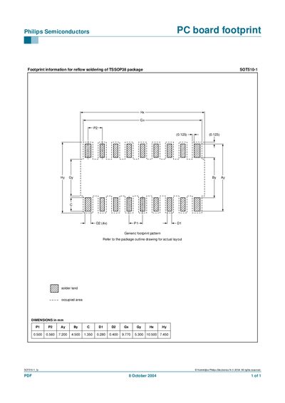
This document supplies the printed‑circuit‑board (PCB) footprint information for the Philips SOT510-1 TSSOP38 semiconductor package. It includes the generic footprint pattern and the dimensions required for accurate layout and reflow soldering.
The table lists key measurements such as pad pitch, pad length, and pad width in millimetres, along with the recommended solder paste density (D2 = 4%). Use these values when designing the board to ensure proper component placement and reliable solder joints.
The generic footprint pattern is provided in the document with all required dimensions for the PCB layout.