
This document is about the dimension information of the PC board footprint of SOT190-1.
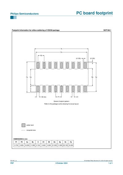
This document supplies the footprint information required for reflow soldering of the VSO56 package identified as SOT190-1. It includes the recommended pad dimensions, spacing, and solder mask openings for designing a printed circuit board that accommodates this component.
The listed dimensions are given in millimetres and should be used together with the package outline drawing for the final layout. Generic footprint patterns are also shown for reference.
| P1 pitch | 0.750 mm |
|---|---|
| P2 pitch | 0.825 mm |
| Ay | 16.200 mm |
| By | 11.900 mm |
| C | 2.150 mm |
| D1 | 0.450 mm |
| D2 | 0.600 mm |
| Gx | 21.250 mm |
| Gy | 11.600 mm |
| Hx | 22.100 mm |
| Hy | 16.450 mm |
It is for the VSO56 package identified as SOT190-1.
Refer to the package outline drawing for the actual layout.