
This is a technical manual about SOT687-1 FOOTPRINT (REFLOW SOLDERING)
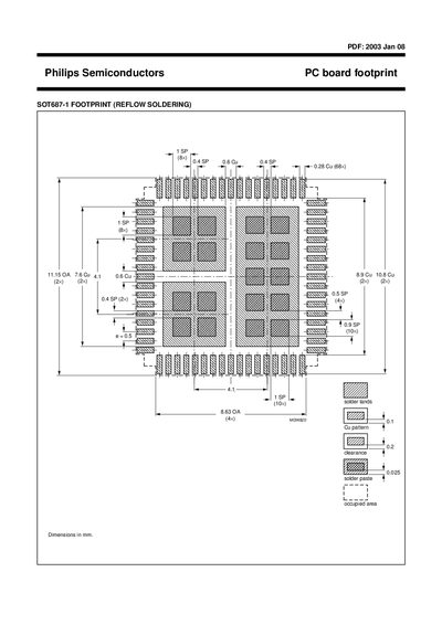
This one‑page document shows the PCB footprint for the Philips SOT687-1 semiconductor package, intended for use with reflow soldering processes. It includes the layout of solder lands, clearance values and occupied area.
All dimensions are expressed in millimetres, and the drawing lists the copper thickness and spacing required for proper assembly. The footprint can be used directly in PCB CAD tools to ensure correct pad placement. This manual is written in Japanese.
| Footprint type | SOT687-1 |
|---|---|
| Dimensions unit | mm |
The document provides the SOT687-1 footprint for reflow soldering.
Dimensions are expressed in millimetres.