
This document is a PDF file that introduces the dimensions, occupied area and soldering information of SOT803-1 products.
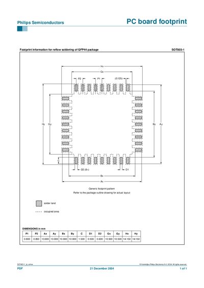
This document describes the recommended PCB footprint for the Philips SOT803-1 semiconductor device. It includes the generic footprint pattern and the dimensions needed for accurate reflow soldering of the QFP44 package.
The footprint dimensions are given in millimetres, with pad pitches, land sizes and overall outline measurements. Users should refer to the package outline drawing for the exact layout before applying the generic pattern to their board designs.
| Package outline dimensions | 13.900 mm × 10.900 mm |
|---|---|
| Pad pitch (P2) | 0.800 mm |
| Pad width (Ax) | 0.500 mm |
The SOT803-1 uses a QFP44 package.
Use the generic footprint pattern with the dimensions listed in the document.