
The MGFC40V5964 is an internally impedance-matched GaAs power FET designed for use in 5.9 - 6.4 GHz band amplifiers. It features high output power, high power gain, high power added efficiency, and low distortion.
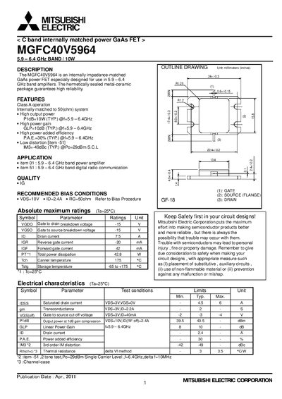
The MGFC40V5964 is a C‑band internally impedance‑matched GaAs power FET designed for use in 5.9‑6.4 GHz band amplifiers. It is supplied in a hermetically sealed metal‑ceramic package for high reliability.
Key specifications include 10 W typical output power, 10 dB typical gain, 30 % typical power‑added efficiency, and a typical third‑order intermodulation distortion of –49 dBc. Recommended bias conditions are VDS = 10 V, ID = 2.4 A, and RG = 500 Ω. Absolute maximum ratings and detailed electrical characteristics are provided for safe circuit design.
| Frequency band | 5.9‑6.4 GHz |
|---|---|
| Typical output power | 10 W |
| Typical gain | 10 dB |
| Typical power‑added efficiency (PAE) | 30 % |
| Typical IM3 | -49 dBc |
| Gate‑to‑drain breakdown voltage (V_GDO) | 15 V |
| Gate‑to‑source breakdown voltage (V_GSO) | 15 V |
| Drain current (ID) max | 7.5 A |
| Forward gate current (I_GF) | 42 mA |
| Reverse gate current (I_GR) | -20 mA |
| Total power dissipation (P_T) | 42.8 W |
| Storage temperature range | -65 °C to +175 °C |
| Junction temperature limit | 175 °C |
It operates in the 5.9‑6.4 GHz band.
The typical output power is 10 W at 5.9‑6.4 GHz.
Recommended bias is VDS = 10 V, ID = 2.4 A, and RG = 500 Ω.
Both the gate‑to‑drain and gate‑to‑source breakdown voltages are rated at 15 V.