
Key facts
- Brand
- STMicroelectronics
- Model
- PSD935G2
- Industry
- Industrial
- Documents
- 2
- Languages
- EN
- Last added
- 2012-06-04
Start here
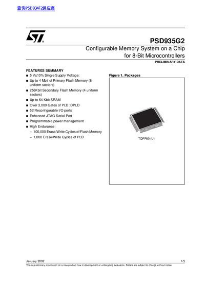
ST PSD935G2 Configurable Memory System on a Chip for 8-Bit Microcontrollers PRELIMINARY DATA
The PSD935G2 is a configurable memory system on a chip (SoC) designed for 8‑bit microcontrollers. It integrates up to 4 Mbit of primary Flash, 256 Kbit secondary Flash, 64 Kbit SRAM, more than 3 000 PLD gates and 52 reconfigurable I/O ports, all powered from a single 5 V supply. The device supports both JTAG‑based In‑System Programming (ISP) and In‑Application Re‑Programming (IAP) for flexible firmware updates.
The architecture includes a Decode PLD for address decoding, a General‑Purpose PLD for custom logic, a built‑in JTAG serial port, an internal page register for address expansion, and a Power Management Unit with an automatic power‑down mode. Pin‑level details, programming methods, and ordering information are provided throughout the document.
STMicroelectronics PSD935G2 specifications
| Primary Flash Memory | 4 Mbit |
|---|---|
| Secondary Flash Memory | 256 Kbit |
| SRAM | 64 Kbit |
| PLD Gate Count | >3 000 gates |
| Reconfigurable I/O Ports | 52 pins |
| Supply Voltage | 5 V ±10 % |
| Standby Current | 50 µA (typical) |
| PLD Erase/Write Cycles | ≥1 000 |
| Package | 80‑pin TQFP |
Source: ST PSD935G2 Configurable Memory System on a Chip for 8-Bit Microcontrollers PRELIMINARY DATA
All STMicroelectronics PSD935G2 documents by type
Ratings, dimensions and ordering codes, for selection and design work.
Questions answered in these manuals
How can the PSD935G2 be programmed without a microcontroller?
It includes a built‑in JTAG‑compliant serial port that allows full‑chip In‑System Programming (ISP) via the JTAG pins on Port E.
From: ST PSD935G2 Configurable Memory System on a Chip for 8-Bit Microcontrollers PRELIMINARY DATA
How does In‑Application Re‑Programming (IAP) work on the PSD935G2?
The main Flash can be programmed in‑system by the MCU while it runs code from the secondary Flash or SRAM, allowing concurrent operation and firmware updates.
From: ST PSD935G2 Configurable Memory System on a Chip for 8-Bit Microcontrollers PRELIMINARY DATA
What is the flash memory endurance of the PSD935G2?
The flash memory is rated for a minimum of 100 000 erase/write cycles.
From: STMicroelectronics PSD935G2 Configurable Memory System Chip Datasheet
How many I/O pins does the PSD935G2 provide?
The device provides 52 individually configurable I/O pins distributed across seven ports.
From: STMicroelectronics PSD935G2 Configurable Memory System Chip Datasheet