
PSD935G2 is a configurable memory system on a chip that includes up to 4 Mbit of primary memory, 256 Kbit of secondary memory, 64 Kbit of SRAM, 3,000 gates of PLD, 52 reconfigurable I/O ports, enhanced JTAG serial port, programmable power management, etc.
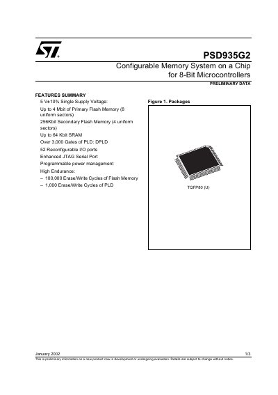
The PSD935G2 Configurable Memory System on a Chip provides a single‑supply 5 V solution for 8‑bit microcontrollers. It integrates up to 4 Mbit of primary flash memory, a 256 Kbit secondary flash for boot or data, 64 Kbit SRAM, more than 3 000 PLD gates and 52 reconfigurable I/O pins, all in an 80‑pin TQFP package. The device includes an enhanced JTAG serial port and a programmable power‑management unit, with low standby current (≈50 µA) and high endurance (≥100 000 flash erase/write cycles).
Programming can be performed via In‑System Programming (ISP) using the IEEE 1149.1‑compliant JTAG interface, allowing the entire device to be programmed while soldered to a board without MCU involvement. In‑Application Re‑Programming (IAP) lets the MCU program one flash array while executing code from the other, enabling field firmware updates. Detailed pin descriptions, bus interface options, and power‑down features are provided for designers.
| Primary Flash Memory | 4 Mbit (8 uniform sectors) |
|---|---|
| Secondary Flash Memory | 256 Kbit (4 uniform sectors) |
| SRAM | 64 Kbit |
| PLD Logic Gates | over 3 000 gates |
| Reconfigurable I/O Ports | 52 ports |
| Supply Voltage | 5 V ±10 % |
| Standby Current | as low as 50 µA (5 V devices) |
| Flash Endurance | ≥100 000 erase/write cycles |
| PLD Endurance | ≥1 000 erase/write cycles |
| Package | 80‑pin TQFP |
The flash memory is rated for a minimum of 100 000 erase/write cycles.
The device provides 52 individually configurable I/O pins distributed across seven ports.