
SSM3K15FU is a TOSHIBA field effect transistor suitable for high-speed switching and analog switch applications. It features a small package and low on-resistance.
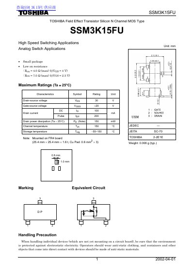
This document is a technical datasheet for the Toshiba SSM3K15FU, an N-channel silicon field effect transistor designed for high-speed switching applications. It provides comprehensive specifications including maximum ratings, electrical characteristics such as on-resistance and capacitance, and typical performance curves under various conditions.
The datasheet includes specific handling precautions regarding electrostatic discharge (ESD) protection and outlines restrictions on product use, advising against application in safety-critical systems like medical instruments or transportation controls without additional customer verification.
| Drain-source voltage (Vdss) | 30 V |
|---|---|
| Gate-source voltage (Vgss) | +20 V |
| Drain current (Idc) | 100 mA |
| Pulse Drain current (Ipp) | 200 mA |
| Drain power dissipation (Ta = 25°C) | 150 mW |
| Channel temperature (Tch) | 150 °C |
| Storage temperature (Tstg) | -55~150 °C |
| Gate threshold voltage (Vth) Min | 0.8 V |
| Drain-source ON resistance (Rds(on)) Max @ Vgs=4V | 4.0 Ω |
| Drain-source ON resistance (Rds(on)) Max @ Vgs=2.5V | 7.0 Ω |
A recommended gate-source voltage of 2.5 V or higher is required to turn on this product.
The maximum drain-source voltage rating is 30 V.
The maximum power dissipation is 150 mW at an ambient temperature of 25°C.
A gate-source voltage of 2.5 V or higher is recommended to turn on this product.