
This document is about CDC950 clock synthesizer/driver, which can generate 8 host clock (100/133 MHz) clocks, 1 CLK33 clock (3.3V, 33.3MHz), 1 REFCLK clock (3.3V, 14.318MHz) and 2 3V48 clocks (3.3V, 180° shifted pairs, 48MHz)
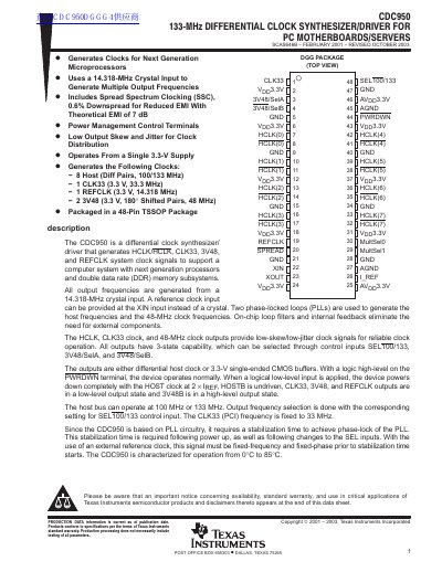
The CDC950 is a differential clock synthesizer and driver designed to generate system clock signals for next-generation microprocessors and DDR memory subsystems. It operates from a single 3.3-V supply and uses a 14.318-MHz crystal input to generate multiple output frequencies, including 100/133 MHz host clocks, 33 MHz PCI clocks, and 48 MHz USB clocks.
The device includes on-chip loop filters and internal feedback, eliminating the need for external components. It features spread spectrum clocking (SSC) with up to 0.6% downspread to reduce EMI and offers low output skew and jitter for reliable clock distribution. The CDC950 is available in a 48-pin TSSOP package and is characterized for operation from 0°C to 85°C.
| Supply Voltage | 3.3 V |
|---|---|
| Crystal Input Frequency | 14.318 MHz |
| Host Clock Frequencies | 100 MHz or 133 MHz |
| Package Type | 48-Pin TSSOP |
No, on-chip loop filters and internal feedback eliminate the need for external components.
The CDC950 is characterized for operation from 0°C to 85°C.
When a logical low-level input is applied to the PWRDWN terminal, the device powers down completely with the HOST clock at 2 x IREF, HOSTB is undriven, CLK33, 3V48, and REFCLK outputs are in a low-level output state and 3V48B is in a high-level output state.