
FDS9933BZ is a dual P-channel 2.5V specified PowerTrench® MOSFET, with low RDS(on), low gate charge, high performance trench technology and HBM ESD protection
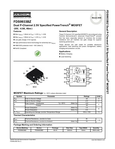
This document is a technical datasheet for the Fairchild Semiconductor FDS9933BZ, a dual P-Channel MOSFET utilizing advanced PowerTrench technology. The device is specified for 2.5V gate drive operation with a maximum on-resistance of 46mΩ at Vgs = -4.5V and Id = -4.9A.
The datasheet provides comprehensive electrical characteristics, including off-state breakdown voltage, threshold voltage, switching times, and capacitance values. It also details thermal resistance ratings for various mounting conditions and includes typical performance curves such as on-resistance versus junction temperature and safe operating areas.
| Drain to Source Voltage (Vds) | -20 V |
|---|---|
| Gate to Source Voltage (Vgs) | +12 V |
| Pulsed Drain Current | -30 A |
| Power Dissipation (Ta = 25°C) | 1.6 W |
| Operating Junction Temperature Range | -55 to +150 °C |
| Thermal Resistance, Junction to Case (RθJC) | 40 °C/W |
| Static Drain to Source On Resistance (Vgs = -2.5V) | 54 mΩ |
| Total Gate Charge (Qg) | 15 nC |
The device supports a maximum continuous drain current of -4.9 A when the temperature is 25°C.
The device operates and stores within a junction temperature range of -55 to +150 °C.
The maximum power dissipation is 1.6 W when the device is mounted on a 2 oz copper pad.