
The document describes a product with the following characteristics: 1. Drain-Source Breakdown Voltage (VGS = 0V, ID = 250µA); 2. Drain-Source On-State Resistance (VGS = 10V, 2A); 3. Zero Gate Voltage Drain Current (VDS = 1000V, VGS = 0V); 4. Zero Gate Voltage Drain Current (VDS = 800V, VGS = 0V, TC = 125°C); 5. Gate-Source Leakage Current (VGS = ±30V, VDS = 0V); 6. Gate Threshold Voltage (VDS = VGS, ID = 1mA).
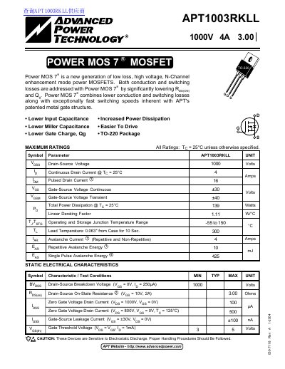
This document is a technical datasheet for the APT1003RKLL, an N-Channel enhancement mode Power MOSFET from Advanced Power Technology. The device is designed as a new generation of low loss, high voltage components with significantly lowered conduction and switching losses.
The datasheet provides maximum ratings, static electrical characteristics, dynamic characteristics including gate charges and switching energies, source-drain diode specifications, thermal characteristics, and typical performance curves such as transfer characteristics and safe operating areas.
| Drain-Source Voltage | 1000 Volts |
|---|---|
| Continuous Drain Current | 4 Amps |
| Total Power Dissipation | 139 Watts |
| Operating Junction Temperature Range | -55 to 150 °C |
| Drain-Source On-State Resistance | 3.00 Ohms |
| Package Type | TO-220 Package |
The total power dissipation is rated at 139 Watts when the case temperature is 25°C.
The device can operate and store within a junction temperature range of -55 to 150 °C.