
This document describes the features and characteristics of the FDMS86520 N-Channel PowerTrench® MOSFET, including maximum on-resistance, advanced package and silicon combination, next generation enhanced body diode technology, 100% UIL testing, etc.
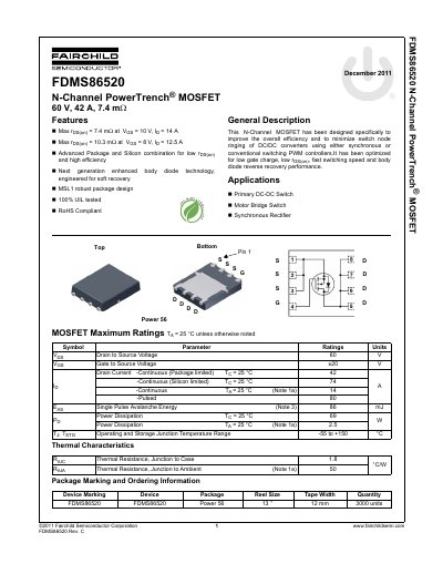
This document is a datasheet for the Fairchild Semiconductor FDMS86520, an N-Channel PowerTrench MOSFET. The device is engineered for soft recovery and is optimized for low gate charge, low on-resistance, and fast switching speed. It is specifically designed to improve the overall efficiency and minimize switch node ringing of DC/DC converters using either synchronous or conventional switching PWM controllers.
| Drain to Source Voltage | 60 V |
|---|---|
| Continuous Drain Current (Package limited) | 42 A |
| Continuous Drain Current (Silicon limited) | 74 A |
| Power Dissipation (Ta = 25°C) | 69 W |
| Operating and Storage Junction Temperature Range | -55 to +150 °C |
| Thermal Resistance, Junction to Case | 18 °C/W |
| Thermal Resistance, Junction to Ambient | 50 °C/W |
| Reverse Recovery Time (Id=14A, di/dt=100 A/µs) | 60 ns |
The device is designed for use as a primary DC-DC switch, a motor bridge switch, and a synchronous rectifier.
The maximum continuous drain current is 42 A when package limited at Ta = 25°C.
Yes, the document states that the device is RoHS Compliant.
The thermal resistance from junction to case is 18 °C/W.