
This datasheet provides the parameters of FDD86326 N-Channel PowerTrench® MOSFET, including maximum voltage, maximum current, maximum resistance, etc.
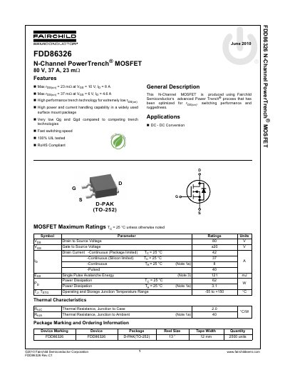
The document describes the Fairchild Semiconductor FDD86326, an N-Channel PowerTrench MOSFET optimized for low on-resistance and switching performance. It is designed for high power and current handling capabilities within a widely used surface mount D-PAK (TO-252) package.
Key features include extremely low gate charge compared to competing trench technologies and fast switching speeds. The device is RoHS compliant and intended for applications such as DC-DC conversion.
| Drain to Source Voltage | 80 V |
|---|---|
| Continuous Drain Current (Package limited) | 42 A |
| Continuous Drain Current (Silicon limited) | 37 A |
| Power Dissipation (Te = 25°C) | 62 W |
| Operating and Storage Junction Temperature Range | -55 to +150 °C |
| Thermal Resistance (Junction to Case) | 2.0 C/W |
| Package Type | D-PAK (TO-252) |
The maximum continuous drain current is 42 A when package limited at Te = 25°C.
The device operates and stores within a junction temperature range of -55 to +150 °C.
Yes, the datasheet lists the device as RoHS Compliant.