
This is the datasheet of FDG6320C, it is a dual N-type and P-type channel digital FET. It has a very small package outline SC70-6, very low gate drive requirements, allowing direct operation in 3V circuits (VGS(th) < 1.5 V), Gate-Source Zener for ESD ruggedness (> 6kV Human Body Model).
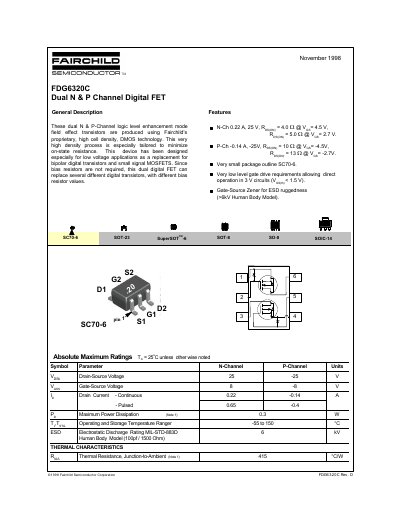
The Fairchild FDG6320C is a dual digital FET produced using proprietary DMOS technology to minimize on-state resistance. It is specifically designed as a replacement for bipolar digital transistors and small signal MOSFETS in low voltage circuits, eliminating the need for bias resistors.
The device features very low gate drive requirements allowing direct operation in 3 V circuits (Vgs < 1.5 V) and includes Gate-Source Zeners for ESD ruggedness exceeding 6kV Human Body Model. It is available in a very small SC70-6 package outline.
| N-Channel Drain Current (Continuous) | 0.22 A |
|---|---|
| P-Channel Drain Current (Continuous) | -0.14 A |
| N-Channel Drain-Source Voltage | 25 V |
| P-Channel Drain-Source Voltage | -25 V |
| Maximum Power Dissipation | 0.3 W |
| Operating and Storage Temperature Range | -55 to 150 °C |
| ESD Electrostatic Discharge Rating | 6 kV Human Body Model |
The device supports a continuous drain current of 0.22 A for the N-Channel and -0.14 A for the P-Channel.
The maximum power dissipation is rated at 0.3 W.
The device operates and stores within a temperature range of -55 to 150 °C.