
This document describes the FDC6561AN Dual N-Channel Logic Level PowerTrenchTM MOSFET, released in April 1999. The product features a continuous drain current of 2.5A and a drain-source voltage of 30V. It is produced using Fairchild Semiconductor's advanced PowerTrench process, which minimizes on-state resistance and gate charge for superior switching performance. The MOSFET is well-suited for applications requiring small size and low-cost DC/DC conversion in battery-powered systems.
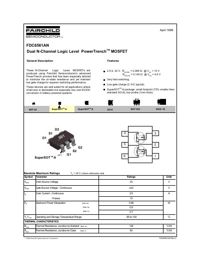
The FDC6561AN is a dual N-channel logic level MOSFET produced using Fairchild Semiconductor's advanced PowerTrench process. It is designed to minimize on-state resistance while maintaining low gate charge for superior switching performance, making it well-suited for small size applications and low cost DC/DC conversion in battery powered systems.
The device features a SuperSOT-6 package with a small footprint and low profile. Key electrical characteristics include a drain-source breakdown voltage of 30V, a continuous drain current of 2.5A, and a typical total gate charge of 2.1nC. It operates over a temperature range of -55 to 150°C.
| Drain-Source Voltage | 30 V |
|---|---|
| Gate-Source Voltage | +20 V |
| Continuous Drain Current | 2.5 A |
| Pulsed Drain Current | 10 A |
| Maximum Power Dissipation | 0.96 W |
| Operating Temperature Range | -55 to 150 °C |
| Thermal Resistance Junction-to-Ambient | 130 °C/W |
| Thermal Resistance Junction-to-Case | 60 °C/W |
| Total Gate Charge | 2.1 nC |
| Package Type | SuperSOT-6 |
The device supports a continuous drain current of 2.5 A.