
FDC6506P is a P-channel logic level MOSFET produced by Fairchild Semiconductor. It is produced using Fairchild Semiconductor's advanced PowerTrench process and has low on-state resistance and low gate charge. It is suitable for applications such as load switch, battery protection and power management.
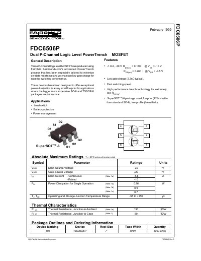
This document is a datasheet for the Fairchild Semiconductor FDC6506P, a dual P-Channel logic level MOSFET produced using the PowerTrench process. The device is designed to offer exceptional power dissipation in a small SuperSOT-6 footprint, making it suitable for applications where larger packages are impractical. Key features include a low on-state resistance of 9-280 mΩ and a low gate charge of 2.3 nC typical.
| Drain-Source Voltage | -30 V |
|---|---|
| Drain Current (Continuous) | -1.8 A |
| On-State Resistance | 9-280 mΩ |
| Gate Charge | 2.3 nC typical |
| Package Type | SuperSOT-6 |
| Operating Temperature Range | -55 to +150 °C |
| Thermal Resistance (Junction-to-Ambient) | 130 °C/W |
The device is designed for applications such as load switches, battery protection, and power management.
The SuperSOT-6 package has a small footprint that is 72% smaller than a standard SO-8 package.
The operating and storage junction temperature range is from -55 to +150 °C.