
This is a document about FDP7030BL/FDB7030BL N-Channel Logic Level PowerTrench MOSFET. The product is designed to improve the overall efficiency of DC/DC converters using either synchronous or conventional switching PWM controllers. These MOSFETs have faster switching and lower gate charge compared to other MOSFETs with similar RDS(ON) specifications. This results in a MOSFET that is easier and safer to drive (even at very high frequencies), and DC/DC power supply designs with higher overall efficiency. It has been optimized for low gate charge, low RDS(ON), and fast switching speed.
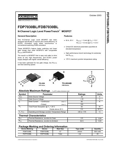
The document describes the FDP7030BL and FDB7030BL as N-Channel Logic Level PowerTrench MOSFETs optimized for low gate charge, low RDS(ON), and fast switching speed. These features are designed to improve the overall efficiency of DC/DC converters using synchronous or conventional switching PWM controllers.
| Drain-Source Voltage (VDSS) | 30 V |
|---|---|
| Gate-Source Voltage (VGSS) | ± 20 V |
| Continuous Drain Current (ID) | 60 A |
| Total Power Dissipation @ TC = 25 °C | 60 W |
| Operating Junction Temperature Range (TJ) | -65 to +175 °C |
| Thermal Resistance, Junction-to-Case (RθJC) | 2.5 °C/W |
| Static Drain–Source On–Resistance @ VGS = 10 V | 9 mΩ |
| Static Drain–Source On–Resistance @ VGS = 4.5 V | 12 mΩ |
| Total Gate Charge (Qg) | 24 nC |
The maximum junction temperature rating is 175°C.
It is designed specifically to improve the overall efficiency of DC/DC converters using either synchronous or conventional switching PWM controllers.
The device marking for the FDB7030BL is 'FDB7030BL'.