
FDB52N20 is a 200V N-channel MOSFET with a low on-state resistance of RDS(on) = 0.049Ω@VGS = 10V, low gate charge (typical 49 nC), low Crss (typical 66 pF), fast switching, 100% avalanche tested, and improved dv/dt capability.
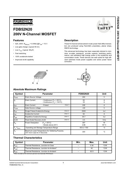
This document is a datasheet for the Fairchild Semiconductor FDB52N20 UniFET, a 200V N-Channel enhancement mode power field effect transistor. The device utilizes proprietary planar stripe DMOS technology to minimize on-state resistance and provide superior switching performance for high efficiency switched mode power supplies and active power factor correction applications.
The datasheet provides comprehensive electrical characteristics, including absolute maximum ratings, off and on characteristics, dynamic parameters, and switching characteristics. It also includes typical performance characteristics graphs, test circuit diagrams, and mechanical dimensions for the TO-263 package.
| Drain-Source Voltage | 200 V |
|---|---|
| Continuous Drain Current (Tg = 25°C) | 52 A |
| Continuous Drain Current (Tg = 100°C) | 33 A |
| Gate-Source Voltage | +30 V |
| Single Pulsed Avalanche Energy | 2520 mJ |
| Power Dissipation (Tc = 25°C) | 357 W |
| Operating and Storage Temperature Range | -55 to +150 °C |
| Thermal Resistance, Junction-to-Case | 0.35 °C/W |
| Package Type | TO-263 |
The device supports a maximum continuous drain current of 52 A when the temperature is 25°C.
It can handle a single pulsed avalanche energy of up to 2520 mJ under specified test conditions.
The absolute maximum gate-source voltage is rated at +30 V.