
This document describes the features and characteristics of the FDB33N25 / FDI33N25 250V N-Channel MOSFET, including 33A current, 250V voltage, low gate charge, and low Crss.
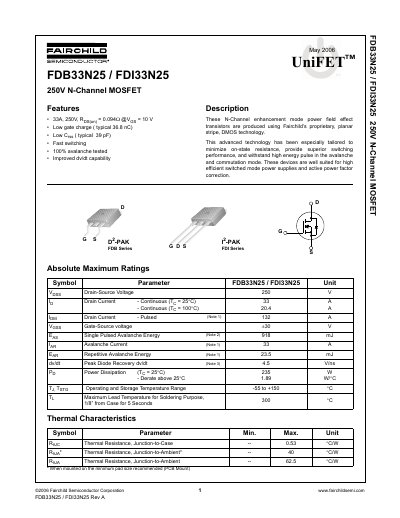
This datasheet describes the FDB33N25 and FDI33N25 N-Channel enhancement mode power field effect transistors produced using Fairchild's proprietary UniFET™ planar stripe, DMOS technology. These devices are designed to minimize on-state resistance and provide superior switching performance, making them well-suited for high-efficiency switched mode power supplies and active power factor correction applications.
| Drain-Source Voltage | 250 V |
|---|---|
| Continuous Drain Current (25°C) | 33 A |
| Continuous Drain Current (100°C) | 20.4 A |
| Pulsed Drain Current | 132 A |
| Power Dissipation (25°C) | 235 W |
| Operating Temperature Range | -55 to +150 °C |
| Package Type (FDB33N25) | D2-PAK |
| Package Type (FDI33N25) | 12-PAK |
The device supports a continuous current of 33 A at 25°C and reduces to 20.4 A when the temperature reaches 100°C.
The FDB33N25 / FDI33N25 can withstand a single pulsed avalanche energy of up to 918 mJ.
The device has a maximum power dissipation rating of 235 W when the case temperature is 25°C.