
This document describes Fairchild Semiconductor's FDC6318P Dual P-Channel 1.8V PowerTrench MOSFET. The product is produced using advanced PowerTrench process, which minimizes on-state resistance and maintains low gate charge for superior switching performance.
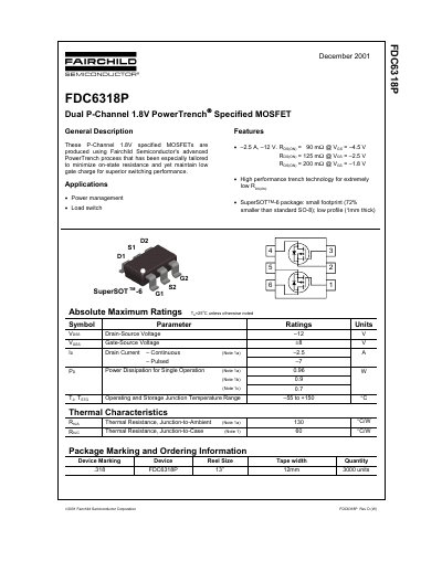
The document describes the Fairchild FDC6318P, a Dual P-Channel 1.8V specified MOSFET produced using the advanced PowerTrench process. This technology is tailored to minimize on-state resistance while maintaining low gate charge for superior switching performance.
Key features include high-performance trench technology and availability in the SuperSOT™-6 package, which offers a small footprint (72% smaller than standard SO-8) and a low profile of 1mm thick. The device is intended for applications such as power management and load switches.
| Drain-Source Voltage (V_DSS) | -12 V |
|---|---|
| Gate-Source Voltage (V_GSS) | +8 V |
| Continuous Drain Current (I_D) | -2.5 A |
| Power Dissipation (Single Operation) | 0.96 W |
| Operating Junction Temperature Range | -55 to +150 °C |
| Package Type | SuperSOT™-6 |
The device supports a continuous drain current of -2.5 A.
The package has a low profile that is 1mm thick.