
FDC6303N is a dual N-channel logic level enhancement mode field effect transistor produced using Fairchild's proprietary high cell density DMOS technology. It has very low on-state resistance. This device is specially designed for low voltage applications as a replacement for digital transistors in load switching applications. Since bias resistors are not required, this N-channel FET can replace several digital transistors with different bias resistors.
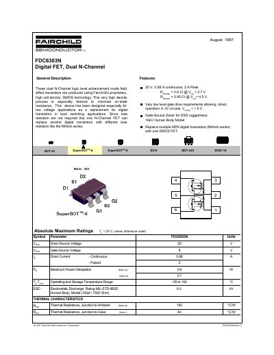
The Fairchild FDC6303N is a dual N-channel logic level enhancement mode field effect transistor produced using Fairchild's proprietary DMOS technology. It is designed for low voltage applications as a replacement for digital transistors in load switching applications, eliminating the need for bias resistors. The device features very low gate drive requirements, allowing direct operation in 8V circuits, and includes a Gate-Source Zener for ESD ruggedness.
| Drain-Source Voltage | 25 V |
|---|---|
| Gate-Source Voltage | 8 V |
| Drain Current - Pulsed | 2 A |
| Maximum Power Dissipation | 0.9 W |
| Operating and Storage Temperature Range | -55 to 150 °C |
| ESD Rating (Human Body Model) | >6kV |
| Thermal Resistance, Junction-to-Ambient | 140 °C/W |
| Thermal Resistance, Junction-to-Case | 60 °C/W |
It is designed especially for low voltage applications as a replacement for digital transistors in load switching applications.
No, since bias resistors are not required, this one N-Channel FET can replace several digital transistors with different bias resistors.
The gate threshold voltage is between 0.65 V and 1.5 V.