
This document describes the features and absolute maximum ratings of the FDC6304P digital FET, a dual P-channel transistor produced in July 1997. It includes parameters such as voltage, current, power dissipation, temperature, etc. The product is manufactured using high-density DMOS technology and has characteristics such as low voltage drive, low on-state resistance, ESD ruggedness, etc. It is suitable for battery-powered applications such as notebook computers and cellular phones.
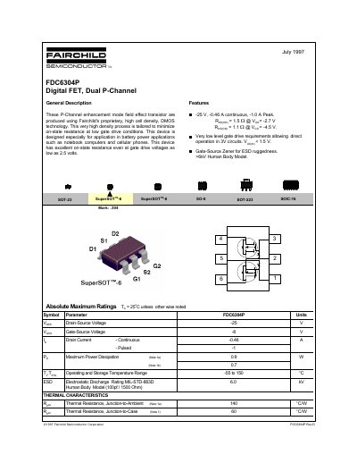
This document is a technical datasheet for the Fairchild Semiconductor FDC6304P, which consists of two P-Channel enhancement mode field effect transistors. The device utilizes high cell density DMOS technology to minimize on-state resistance at low gate drive conditions, making it suitable for battery-powered applications like notebook computers and cellular phones.
The datasheet provides comprehensive electrical characteristics, including absolute maximum ratings such as a drain-source voltage of -25V and continuous drain current of -0.46A. It also details thermal characteristics, switching parameters, and typical performance curves under various operating conditions.
| Drain-Source Voltage (Vss) | -25 V |
|---|---|
| Continuous Drain Current (I) | -0.46 A |
| Peak Drain Current | -1.0 A |
| Maximum Power Dissipation (Note 1a) | 0.9 W |
| Operating and Storage Temperature Range | -55 to 150 °C |
| ESD Rating (Human Body Model) | >6kV |
The device supports a continuous drain current of -0.46 A.
The operating and storage temperature range is -55 to 150 °C.