
fdc6306p is a p-channel 2.5v specified mosfet produced by fairchild semiconductor. it uses fairchild semiconductor's advanced powertrench process, which has the characteristics of low on-state resistance and low gate charge. it is suitable for applications such as load switch, battery protection and power management.
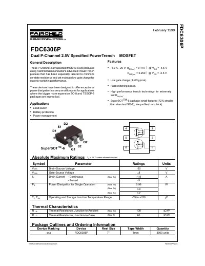
This document is a datasheet for the Fairchild Semiconductor FDC6306P, a dual P-channel MOSFET designed using the PowerTrench process. The device is specified for a 2.5V gate threshold and is packaged in a SuperSOT-6 format, which offers a small footprint and low profile suitable for applications where larger packages are impractical.
The datasheet provides comprehensive electrical characteristics, including absolute maximum ratings, on and off characteristics, dynamic parameters, and switching characteristics. It also includes typical performance curves and ordering information for the device.
| Drain-Source Voltage | -20 V |
|---|---|
| Gate-Source Voltage | +8 V |
| Continuous Drain Current | -19 A |
| Power Dissipation (Single Operation) | 0.96 W |
| Operating Junction Temperature | -55 to +150 °C |
| Thermal Resistance (Junction-to-Ambient) | 130 °C/W |
It is designed for use as a load switch, battery protection, and power management.
The maximum continuous drain current is -19 A.