
FDC6310P is a dual P-channel 2.5V specified MOSFET produced by Fairchild Semiconductor Corporation. It features low on-state resistance and low gate charge, and is suitable for applications such as load switches, battery protection and power management.
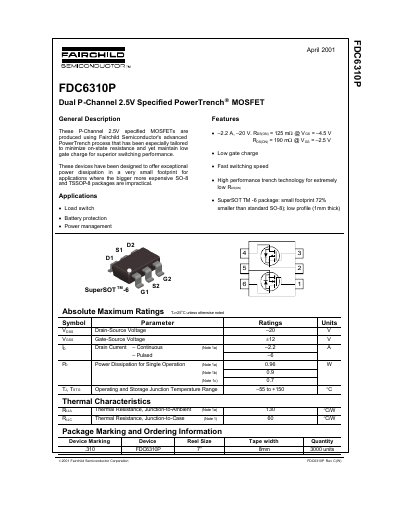
The document describes the Fairchild FDC6310P, which utilizes advanced PowerTrench technology to minimize on-state resistance while maintaining low gate charge for superior switching performance. These devices are designed for applications requiring high power dissipation in a small footprint, such as load switches and battery protection circuits.
| Drain-Source Voltage (Vdss) | -20 V |
|---|---|
| Continuous Drain Current (Ib) | +— 2.2 A |
| Power Dissipation (Single Operation) | 0.96 W |
| Operating Junction Temperature Range | -55 to +150 °C |
| Package Type | SuperSOT™-6 |
This device is designed for use as a load switch, battery protection circuit, or power management component.
The device supports a continuous drain current of 2.2 A under specified conditions.
The component can operate and be stored within a junction temperature range of -55 to +150 degrees Celsius.