
This document describes the features and characteristics of the FDC6320C dual N&P channel digital field effect transistor released in October 1997, including parameters such as operating voltage, maximum power, temperature range, etc. The product has low-level gate drive requirements and can be directly operated in 3V circuits. It is suitable for low voltage applications as a replacement for bipolar digital transistors.
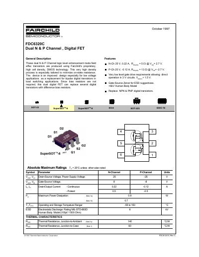
The document describes the Fairchild FDC6320C, a dual digital FET utilizing proprietary DMOS technology. It is specifically tailored to minimize on-state resistance and serves as an improved design for low voltage load switching applications, replacing bipolar digital transistors without requiring bias resistors.
Key features include very low gate drive requirements allowing direct operation in 3 V circuits, ESD ruggedness via a Gate-Source Zener (rated at >6kV Human Body Model), and availability in various packages including SOT-23, SuperSOT™-6, SuperSOT™-8, SOT-223, and SOIC-16.
| N-Ch Drain-Source Voltage | 25 V |
|---|---|
| P-Ch Drain-Source Voltage | -25 V |
| N-Ch Continuous Drain/Output Current | 0.22 A |
| P-Ch Continuous Drain/Output Current | -0.12 A |
| N-Ch On-Resistance (Vgs=2.7V) | 5 Ω |
| P-Ch On-Resistance (Vgs=-2.7V) | 13 Ω |
| Gate-Source Zener Rating | >6kV Human Body Model |
| Operating Temperature Range | -55 to 150 °C |
It is an improved design especially for low voltage applications as a replacement for bipolar digital transistors in load switching applications.
No, since bias resistors are not required, this dual digital FET can replace several digital transistors with difference bias resistors.
The device has very low level gate drive requirements allowing direct operation in 3 V circuits, with Vasu < 1.5 V.