
The document describes the features and characteristics of the 2N7000BU/2N7000TA product, including fast switching times, improved inductive ruggedness, lower input capacitance, extended safe operating area, and improved high temperature reliability.
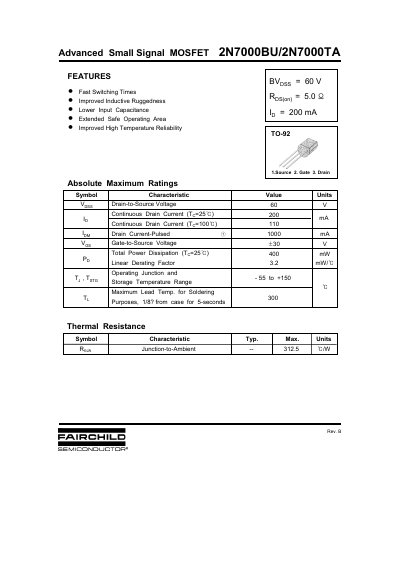
This document is a datasheet for the Fairchild Semiconductor 2N7000BU/2N7000TA, an N-channel small signal MOSFET. Key features include fast switching times, improved inductive ruggedness, and a lower input capacitance. The device is housed in a TO-92 package with pinout defined as Source, Gate, and Drain.
| Drain-to-Source Voltage | 60 V |
|---|---|
| Continuous Drain Current (25°C) | 200 mA |
| Continuous Drain Current (100°C) | 110 mA |
| Pulsed Drain Current | 1000 mA |
| Gate-to-Source Voltage | +30 V |
| Total Power Dissipation (25°C) | 400 mW |
| Operating Junction Temperature Range | -55 to +150 °C |
| Junction-to-Ambient Thermal Resistance | 312.5 °C/W |
The device is packaged in a TO-92 package.
The pinout is defined as 1. Source, 2. Gate, and 3. Drain.
The maximum gate-to-source voltage is +30 V.