
This document describes the features and characteristics of the BSS123 N-Channel Logic Level Enhancement Mode Field Effect Transistor produced by Fairchild Semiconductor Corporation. These products are made using Fairchild's proprietary high cell density DMOS technology, which aims to minimize on-state resistance and provide rugged, reliable, and fast switching performance. These products are particularly suitable for low voltage, low current applications such as small servo motor control, power MOSFET gate drivers, and other switching applications.
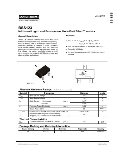
This document is a technical datasheet for the Fairchild Semiconductor BSS123, an N-Channel Logic Level Enhancement Mode Field Effect Transistor. The device utilizes proprietary DMOS technology to minimize on-state resistance while providing rugged and reliable performance for low voltage and low current applications such as servo motor control and power MOSFET gate drivers.
The datasheet provides comprehensive electrical characteristics, including absolute maximum ratings, off and on characteristics, dynamic parameters like capacitance, switching times, and drain-source diode specifications. It also includes typical characteristic curves illustrating on-resistance variation with temperature and current, transfer characteristics, and safe operating areas.
| Drain-Source Voltage (Vdss) | 100 V |
|---|---|
| Gate-Source Voltage (Vgss) | +20 V |
| Operating Junction Temperature Range | -55 to +150 °C |
| Package Type | SOT-23 |
The maximum continuous drain current for the BSS123 is 0.17 A.
The device operates and stores within a junction temperature range of -55 to +150 °C.
The maximum power dissipation for this transistor is 0.36 W.