
The document describes a typical half-bridge driver with features such as floating channel, positive and negative offset power supply, low di/dt gate driver, and cross-conduction prevention.
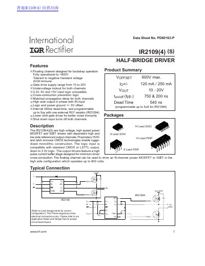
The document describes the IR2109(4)(S), a high voltage, high speed power MOSFET and IGBT driver featuring dependent high and low side referenced output channels. It utilizes proprietary HVIC and latch immune CMOS technologies for ruggedized monolithic construction.
Key features include floating channel design for bootstrap operation up to +600V, tolerance to negative transient voltage, and dV/dt immunity. The device supports gate drive supply ranges from 10 to 20V with undervoltage lockout for both channels.
| High side floating absolute voltage (VB) | -0.3 to 625 V |
|---|---|
| Gate drive supply range | 10 to 20V |
| Undervoltage lockout threshold (positive) | 8.0 V |
| Turn-on propagation delay (typical) | 750 ns |
| Internal dead-time | 540 ns |
| Junction temperature maximum | 150 °C |
The maximum high side floating absolute voltage (VB) is 625 V.
Yes, for the IR21094 variant, the internal 540ns dead-time is programmable up to 5us with one external R DT resistor.
The device is compatible with standard CMOS or LSTTL output down to 3.3V logic.