
This document describes the features and characteristics of the IR2103(S) high voltage, high speed power MOSFET and IGBT drivers, such as floating channel design, bootstrap operation, negative transient voltage immunity, logic compatibility, etc.
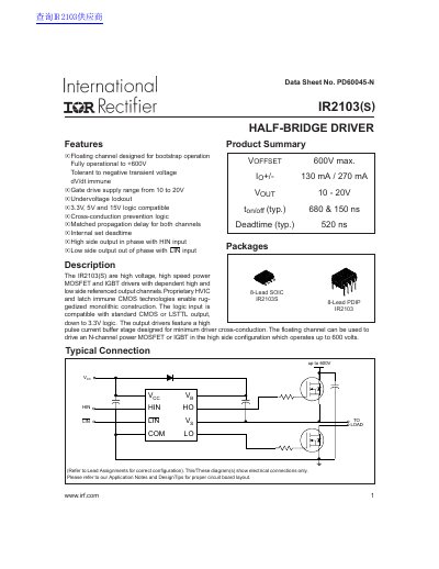
The IR2103(S) is a high voltage, high speed power MOSFET and IGBT driver with dependent high and low side referenced output channels. It utilizes proprietary HVIC and latch immune CMOS technologies for ruggedized monolithic construction. The device is designed for bootstrap operation with a gate drive supply range from 10 to 20V and includes features such as undervoltage lockout, cross-conduction prevention logic, and internal set deadtime.
| High side floating absolute voltage | 625 V |
|---|---|
| High side floating supply offset voltage | 600 V |
| Gate drive supply range | 10 - 20 V |
| Turn-on propagation delay (typ.) | 680 ns |
| Turn-off propagation delay (typ.) | 150 ns |
| Deadtime (typ.) | 520 ns |
| Logic input compatibility | 3.3V, 5V and 15V |
| Package types | 8-Lead SOIC, 8-Lead PDIP |
The maximum high side floating absolute voltage is 625V.
The gate drive supply range is from 10 to 20V.
Yes, the device is tolerant to negative transient voltage.
Yes, it includes cross-conduction prevention logic.