
The IR2112(S) is a high voltage, high speed power MOSFET and IGBT driver with independent high and low side referenced output channels. Proprietary HVIC and latch immune CMOS technologies enable rugge- dized monolithic construction. Logic inputs are com- patible with standard CMOS or LSTTL outputs, down to 3.3V logic. The output drivers feature a high pulse current buffer stage designed for minimum driver cross-conduction. Propagation delays are matched to sim- plify use in high frequency applications. The floating channel can be used to drive an N-channel power MOSFET or IGBT in the high side configuration which operates up to 600 volts.
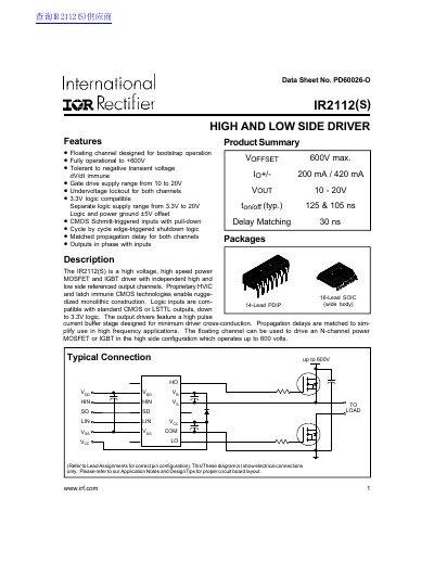
The document is a technical data sheet for the International Rectifier IR2112(S) High and Low Side Driver. This proprietary HVIC utilizes ruggedized monolithic construction and latch immune CMOS technologies to drive N-channel power MOSFETs or IGBTs in high-side configurations up to 600 volts.
| High Side Floating Supply Voltage (Max) | 625 V |
|---|---|
| High Side Floating Supply Offset Voltage (Max) | 600 V |
| Logic Supply Range | 3.3V to 20V |
| Undervoltage Lockout (High Side) | 7.4 V to 9.6 V |
| Turn-On Propagation Delay (Typ) | 125 ns |
| Output High Short Circuit Pulsed Current (Min) | 200 mA |
The absolute maximum rating for the high side floating supply voltage (VB) is 625 V.
The typical turn-on propagation delay (ton) is 125 ns when Vss = 0V.